
This post answers a fairly simple question: how does a person electrically connect a very large number of chips to a very large number of PCBs in the shortest possible amount of time? Without the help of big fancy industrial equipment, that is.
The question is simple, but the answer is far from it. I’ll explain how we do it in this post.
When we first started our shop, we would send out assembled kits to our supporters with the chips fully soldered to the boards. This was fairly straightforward to do, since there weren’t that many of them.
It’s still just Phil and I making PCBs, which we do on a weekly basis, and soldering that many boards is starting to get tricky.
To solve this problem, we decided to approach the problem by using principles of “spring contacts”.
At a very fundamental level, the way that two materials conduct electricity is by physical contact. If the two materials are close enough together, then electricity will flow.
Soldering is a way of bonding two materials together physically, but it isn’t required for two materials to conduct electricity.
If you doubt me, try turning on a light switch or plugging something into an outlet. Those connections, and so many more, aren’t based on soldering, but something else: spring contacts (or spring force).
That’s exactly what it sounds like: the force caused by a spring, which pushes two materials together. The force of that spring pushing the materials together ensures good physical contact, which ensures good electrical flow.
Nothing about this is particularly controversial. There’s no accepted standard between soldering or spring contacts. Which is better simply depends on the application.
Now, I’m going to show you how we use spring contacts to attach optical sensors to PCBs.
The life of a PMW-3360 optical chip starts life looking like this (from the side):
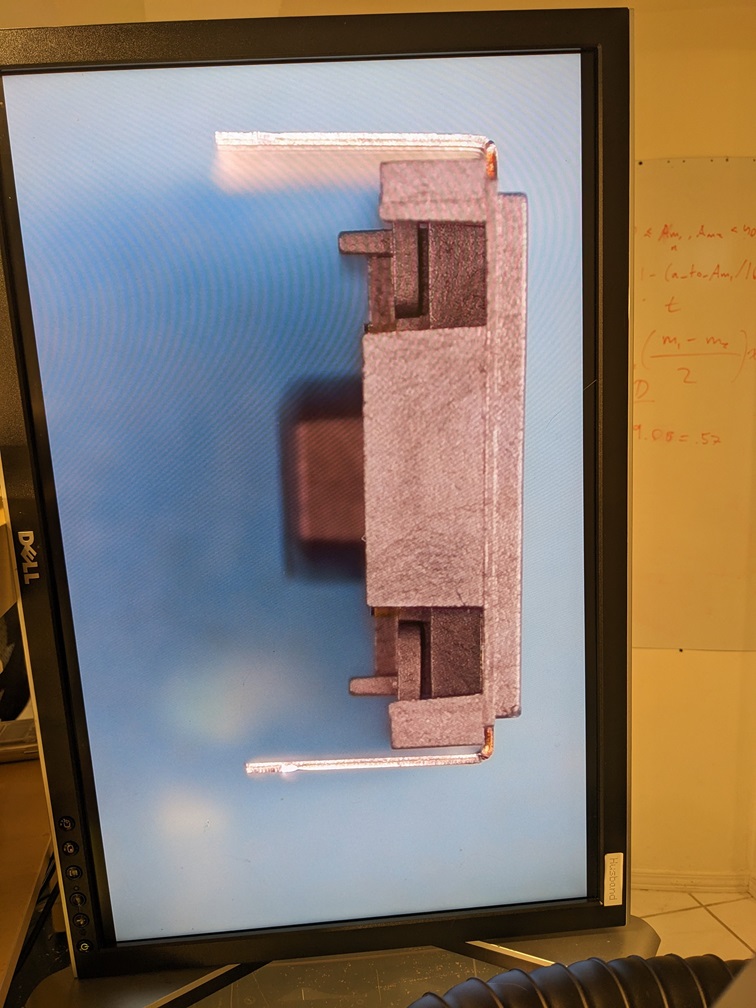
This is a close-up image taken via our rework microscope. You’ll notice that the leads of the chip are at a 90 degree angle from the plane of the sensor.
If we were to put this chip into a PCB, it would likely make very poor electrical contact across all of its pins, if it made any at all. And, it would fall out the second you flip the PCB upside down.
So, we process the chip a bit. It goes into a jig that bends the leads outwards. That process looks like this:
Now, let’s take a look at the PMW-3360 under the microscope again:
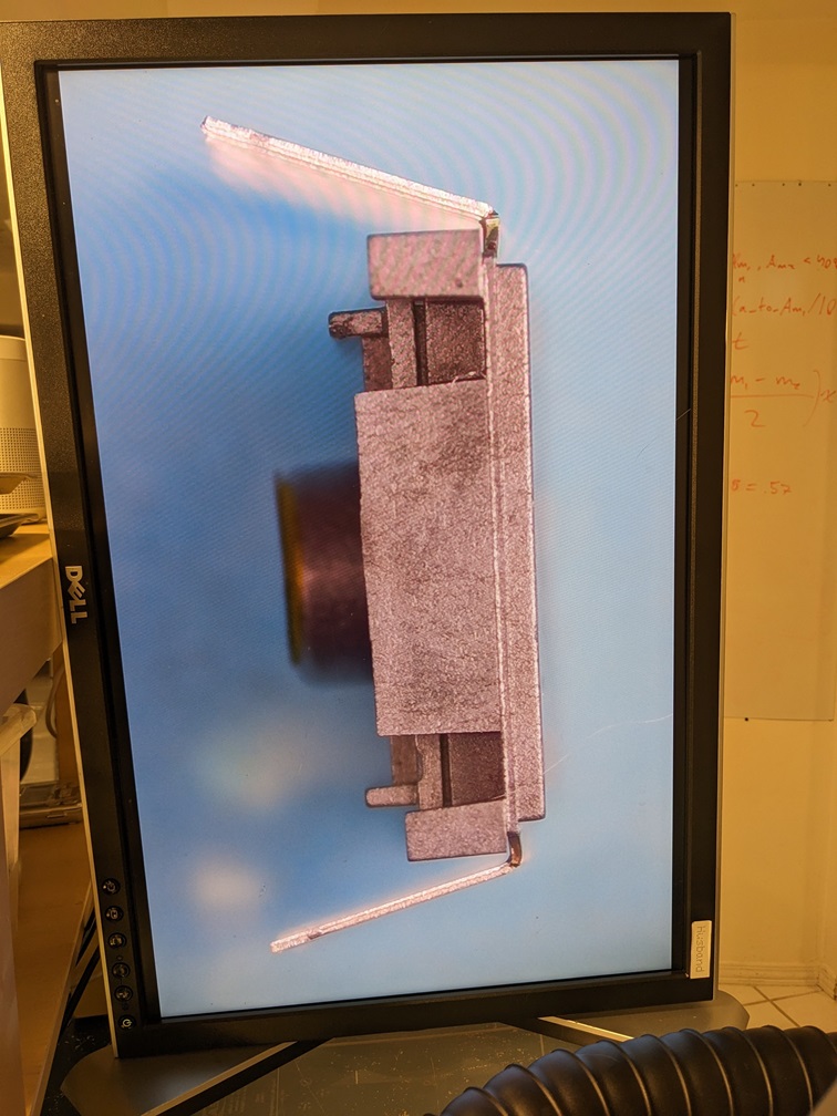
Ah, the leads are bent outwards.
If the chip were to be inserted into a PCB now, then the leads would be pressing against the outside of the holes in which the chip sat. This would cause great physical and electrical contact.
Let’s take another look under the microscope to see what the chip looks like once it’s inserted into the PCB:
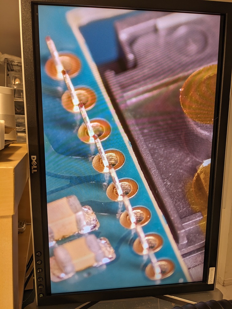
As you can see, the leads are all making contact with the vias.
The question remains: does it work?
We’ve been building and testing mice with the chips inserted in this way for months now, and so far, not a single unit has failed in the field. So, I’d say that’s successful.
So, what are the downsides?
The biggest one is that it’s quite difficult to repair this sort of contact if you don’t have the insertion or bending jig, both of which we designed custom for this process.
Apart from that, there’s lots to like: it’s much faster, much cleaner, and results in good contacts. The chip is also quite difficult (though not impossible) to push out of the PCB, as the spring force also acts to push the chip into the PCB.
We’ll continue building our kits like this for the foreseeable future.